

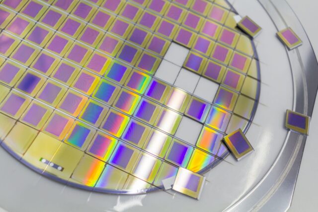
We are surrounded by ever-evolving technology these days. Our everyday life is dependent on hundreds of electronic gadgets. But have you ever stopped to wonder how your phone or laptop works? It isn’t magic, but an equally amazing process: wafer processing.
Cutting-edge technology and detailed accuracy transform raw silicon crystals into complicated integrated circuits in semiconductor manufacture. Wafer processing, a collection of intricate procedures, enables this journey. In this guide, you can deeply dive into the intriguing world of wafer processing and examine how Silyb Wafers convert silicon wafers into the building blocks of today’s electronics.
Starting Point: Silicon Crystals
The silicon crystal, the cornerstone of semiconductor fabrication, is our starting point. The exceptional qualities of silicon, including its abundance, relative simplicity of processing, and ability to carry electricity under particular circumstances, led to its selection.
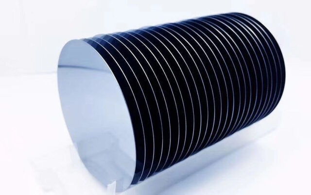
High-purity silicon crystals are made as the first step in producing wafers. The Czochralski method is the method used to do this. A seed crystal is submerged in molten silicon during this procedure. A single, substantial silicon crystal can form due to the delayed removal and rotation of the seed crystal. Then, diamond saws cut this crystal into wafers typically less than a millimeter thick.
Wafer Inspection And Cleaning
The silicon wafers still need to be prepared for semiconductor manufacture after being cut into slices. These wafers must undergo stringent cleaning and inspection procedures to ensure their quality and purity.
Contaminants are cleaned off the wafer surfaces using ultrasonic baths. The wafers are subjected to a series of inspections after washing to find any flaws or contaminants that can impair the performance of the finished semiconductor devices. To preserve the best yield feasible, any defective wafers are eliminated at this point.
Building The Insulating Layers Through Oxidation
The next stage of wafer processing involves coating the silicon wafers with insulating materials. This is accomplished using a procedure known as oxidation. The wafers are heated to high temperatures while exposed to oxygen or steam in the oxidation process. As a result, the wafers’ surface develops a thin layer of silicon dioxide.
As insulators, these silicon dioxide layers enable the uninterrupted development of conductive channels on the silicon. They are essential for isolating various semiconductor chip components.
Making The Patterns In Photolithography
Photolithography is one of the most important processes in wafer processing. This procedure is comparable to creating miniature works of art on silicon canvas.
In photolithography, the surface of the wafer is coated with a photoresist, a light-sensitive substance. The wafer is covered with a mask that has the pattern for the future circuit printed on it. The photoresist is then exposed by shining ultraviolet light through the mask in a particular pattern.
The portions where the circuit should stay can be covered with a protective layer by developing the exposed photoresist. Removing the photoresist’s exposed portions makes the underlying silicon dioxide layer visible.
Etching: Carving The Circuit
Etching selectively removes material from the wafer to define the circuit’s pattern. Two primary types of etching are used in semiconductor manufacturing: wet etching and dry etching.
Wet etching involves using chemical solutions to dissolve the exposed silicon dioxide. Dry etching, on the other hand, uses plasma to remove material. The choice between these two methods depends on the specific requirements of the circuit design and the desired precision.
The etching process is repeated multiple times to create the intricate layers and pathways of the integrated circuit.
Ion Implantation: Functional Doping
Ion implantation is the following procedure in wafer processing. To change the silicon substrate’s electrical characteristics, particular components are implanted during this procedure. The creation of the p-type and n-type regions required for constructing transistors and other semiconductor components depends on this.
Semiconductor makers can precisely tailor the electrical properties of integrated circuits to satisfy the required performance criteria by carefully regulating the type and concentration of dopants implanted into the silicon.
Adding The Layers In Deposition
Deposition is the process of putting small amounts of material in thin layers on the surface of the wafer. This produces insulating layers, conductive routes, and other integral parts of the integrated circuit.
Materials are frequently deposited onto wafers using the processes of chemical vapor deposition (CVD) and physical vapor deposition (PVD). While PVD depends on physical processes like sputtering to create layers, CVD relies on chemical reactions to deposit material.
Surface Smear With Chemical Mechanical Polishing (CMP)
The wafer’s surface may grow uneven as more layers are added. Chemical mechanical polishing (CMP) ensures that ensuing layers are applied precisely and uniformly. This procedure uses chemical reactions and mechanical abrasion to remove extra material and produce a smooth, flat surface.
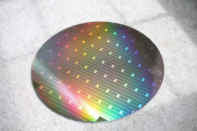
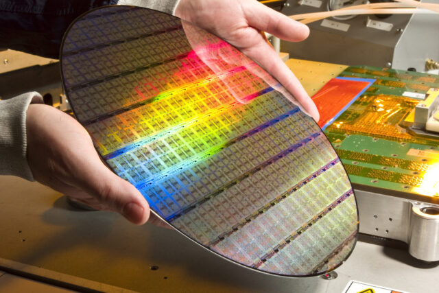
Inspection And Testing At The End
After all the complicated layers and parts have been added, the silicon wafer is examined and tested again. This entails visual inspection to spot any physical flaws and electrical testing to guarantee that the circuit operates as intended.
Only high-quality semiconductor devices go to the following step of manufacturing because any flawed wafers or chips are marked for removal.
Wafer Packaging And Dicing
Cutting the wafer into separate semiconductor chips is the last stage in the wafer processing process. The wafer is divided into individual chips that are generally a few millimeters in size, using diamond saws to cut the wafer along predetermined lines.
The fragile components are then protected from external elements like moisture and dust by protective enclosures providing electrical connections.
Wrapping Up!
From the humble silicon crystal to the intricate integrated circuits that power our modern world, wafer processing is a blend of art and science. It requires precision, creativity, and an unwavering commitment to quality. Every step in the process plays a crucial role in determining the performance and reliability of the final semiconductor devices.
As technology advances, wafer processing techniques evolve, pushing the boundaries of what is possible in electronics. The next time you hold a smartphone or use a computer, take a moment to appreciate the incredible journey from crystals to circuits, all thanks to the intricate world of wafer processing.


